TSMC Debuts A13 Process Technology at 2026 Technology Symposium

On April 22, 2026, TSMC officially introduced its A13 process technology during the company's North America Technology Symposium in Santa Clara, California. The announcement represents the foundry's latest push into second-generation gate-all-around nanosheet transistor technology, positioning itself as a direct optical shrink of the A14 node first revealed in 2025.
The A13 process delivers a 6% reduction in chip area compared to A14 while maintaining full backward compatibility with existing design rules. This compatibility means customers can migrate designs without the painful re-engineering cycles that typically plague node transitions (a problem that has plagued users for years, frankly).
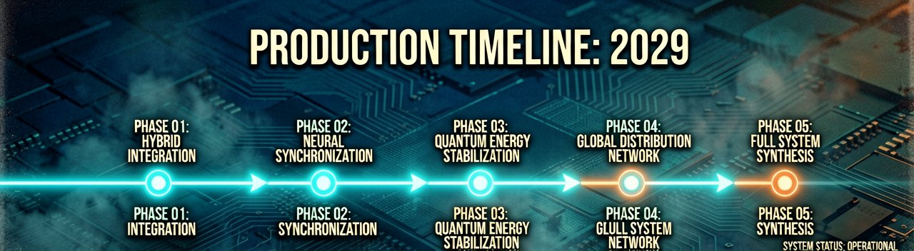
According to the official press release from TSMC, the A13 process is scheduled to enter high-volume production in 2029, one year after the planned A14 ramp. The technology targets next-generation artificial intelligence, high-performance computing, and premium mobile applications where density and power efficiency matter most.
At the symposium, TSMC Chairman and CEO Dr. C.C. Wei emphasized the company's commitment to delivering reliable silicon technology pipelines. "At TSMC, we understand our customers are always looking ahead to their next innovation and they come to us for a reliable stream of new silicon technologies, like A13, meticulously engineered to be ready for high-volume production right when their visionary new designs demand them," Wei stated during the event.
The A13 announcement was part of a broader technology roadmap reveal that included several other advanced nodes and packaging solutions. Senior Vice President Kevin Zhang confirmed that neither A13 nor the companion A12 process will require High-NA EUV lithography tools, relying instead on design-technology co-optimization and existing EUV equipment. This decision avoids the massive capital expenditure associated with next-generation High-NA scanners while continuing aggressive scaling.
Alongside A13, TSMC previewed the A12 process, an A14 derivative optimized specifically for AI and HPC workloads. A12 features Super Power Rail technology for backside power delivery, addressing power integrity constraints that plague data center and HPC applications. Both A12 and A13 are scheduled for 2029 production, though they serve distinctly different market segments.
The company also introduced N2U, an optimized 2nm platform offering 3-4% speed gains or 8-10% power reduction compared to N2P, plus a 1.02-1.03x logic density improvement. N2U leverages the process maturity and strong yield performance of the existing 2nm technology platform, with production expected to start in 2028. This represents a balanced option for AI, HPC, and mobile applications.
What's notable about this roadmap is the deliberate bifurcation of process technology introductions. TSMC is now offering annual node updates for client and mobile applications—prioritizing cost efficiency and IP reuse—while rolling out biennial high-performance nodes for AI and HPC focused on raw performance and backside power delivery. This strategy reflects the shifting revenue dynamics where AI and HPC have begun outpacing traditional smartphone demand.
Advanced packaging received significant attention at the symposium as well. TSMC continues expanding its CoWoS technology to integrate more silicon, now producing 5.5-reticle size CoWoS and planning for even larger versions. A 14-reticle size CoWoS, capable of integrating approximately 10 large compute dies and 20 HBM stacks, is slated for production in 2028. This will be followed by expansion beyond 14 reticles in 2029.
The company also announced TSMC-SoIC 3D chip stacking technology on its most advanced platforms. A14-to-A14 SoIC is expected in 2029, offering 1.8x higher die-to-die I/O density compared with N2-on-N2 SoIC, supporting higher bandwidth data transfer between stacked chips. For automotive applications, N2A—the first automotive process using nanosheet transistors—is expected to achieve AEC-Q100 validation in 2028.
From a physical perspective, these process improvements translate to tangible differences in chip design. Engineers working with A13 will see smaller transistor footprints, reduced routing congestion, and improved thermal characteristics. The 6% area savings might sound modest on paper, but in practice it means more compute units per die, lower per-unit costs, and potentially better power envelopes for mobile devices where battery life is measured in hours rather than days.
Independent reporting from Tom's Hardware corroborates the timeline and technical specifications while adding context about the strategic shift in node development cadence. The outlet notes that this bifurcated approach marks a significant departure from TSMC's historical one-size-fits-all methodology.
The official documentation from TSMC reveals additional details about the technology stack. A13 builds on second-generation GAA nanosheet transistors, achieving enhanced power efficiency and performance through design-technology co-optimization. The process maintains electrical compatibility with A14, meaning voltage levels, timing characteristics, and signal integrity parameters remain consistent across the transition.
For chip designers, the practical implications are straightforward. Existing A14 designs can migrate to A13 with minimal redesign effort, reducing time-to-market for next-generation products. The backward compatibility extends to design rules, PDK structures, and verification flows, which means the learning curve for adoption is relatively shallow compared to previous generational shifts.
However, the 2029 production timeline raises questions about near-term availability. With AI chip demand surging through 2027 and 2028, customers will need to plan their design cycles accordingly. The gap between announcement and production is typical for advanced nodes, but it means that A13 won't be available for the immediate wave of AI infrastructure deployments currently in development.
Whether the industry actually needs another incremental node improvement remains an open question. The semiconductor market has been grappling with diminishing returns from Moore's Law scaling for years, and the economic justification for each new generation becomes increasingly complex. Customers will weigh the 6% area savings against the costs of design migration, verification, and potential yield ramp challenges.
The A13 announcement solidifies TSMC's position in the premium process race, but the real test comes when production begins. Whether customers actually pay for the incremental improvements, or whether the market shifts toward alternative scaling approaches like advanced packaging and chiplet architectures, remains to be seen. Time will tell if this works.
Artūras Malašauskas is an AI Systems Integrator with 20+ years of production-grade web engineering experience. He has designed, shipped, and scaled enterprise Python/PHP systems for logistics, SaaS, and public-sector clients. For the past year, he has focused exclusively on AI integrations: deploying open-source LLMs, building generative media pipelines (image, audio, video), and engineering multi-agent workflows for real production environments. His standard: reproducibility, security, cost-efficient inference—no vaporware. He documents and evaluates emerging AI tooling, separating verified capabilities from marketing noise. Technical editor at: muza-ai.eu, ai-verslas.lt, ai-naujinos.lt Connect on LinkedIn
Comments