The Optical Revolution: Dismantling the GPU Monopoly and Rewiring AI Infrastructure
The artificial intelligence hardware landscape is undergoing a seismic shift as the industry pivots from traditional graphics processing units (GPUs) to next-generation optical computing architectures. For years, the scaling of AI models has relied on squeezing more transistors onto silicon, a strategy now meeting harsh thermodynamic and economic limits. As transformer-based architectures demand exponentially greater computational clusters, the primary bottleneck has shifted from raw chip processing speed to internal input/output (I/O) data transfer constraints. Moving data via traditional copper wiring generates unsustainable thermal loads and energy penalties, forcing hyperscalers to rethink data center architecture from the ground up.
To shatter these physical boundaries, the technology sector is aggressively integrating silicon photonics, replacing copper traces with light-based interconnects that transfer data via laser pulses. This transition promises unprecedented speed and energy efficiency, fundamentally altering how data centers power large-scale machine learning models. By encoding information into multiple wavelengths of light, optical architectures can achieve up to ten times the bandwidth of traditional electrical networks while drawing a fraction of the power. The strategic implications are vast, as the ability to link thousands of individual accelerators into a singular, low-latency computational fabric threatens to dilute the hardware lock-in long enjoyed by dominant GPU manufacturers.
The urgency of this transition is underscored by massive capital reallocation across the semiconductor supply chain. According to reporting by The Next Web, market leaders like Nvidia have committed over $6.5 billion to photonics companies to scale up the optical supply chain and aggressively bypass the looming "copper wall." Concurrently, industry consortia consisting of major hyperscalers and chipmakers have established unified frameworks, such as the Optical Compute Interconnect (OCI) Multi-Source Agreement reported by Lightmatter Blog, advanced 3D photonic interposers can integrate hundreds of optical fibers directly into chip architectures. This layout enables optical I/O platforms to deliver up to 256 Terabits per second (Tbps) of total bandwidth per chip package. By replacing copper wires with light, infrastructure operators can scale cluster communication without facing the catastrophic thermal throttles that plague tightly packed electronic accelerators.
The Rise of Matrix-Multiplication Optical Processors
Beyond simply moving data with light, next-generation architectures are executing mathematical computations in the optical domain. Optical processors manipulate light waves to perform analog matrix-vector multiplications—the fundamental mathematical operation underpinning neural networks—at the speed of light. Because photons pass through optical networks without the resistance encountered by electrons in silicon, these chips perform calculations with near-zero power consumption during propagation.
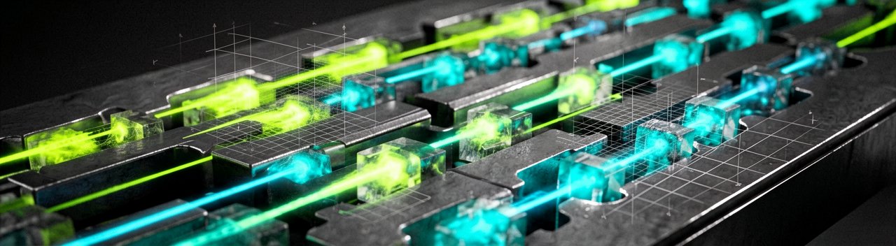
While fully general-purpose optical computers remain a long-term goal, specialized optical accelerators are already targeting AI inference workloads. Companies like Lightelligence are demonstrating innovative product suites that integrate neural network processing with advanced photonic integrated circuit (PIC) switching, as highlighted by Photonic Integrated Circuits Magazine. These specialized hybrid systems handle heavy mathematical sub-routines optically while leaving arbitrary logic to conventional host processors, maximizing the efficiency of complex AI workloads.
Commercial Hurdles and the Road to Mass Production
Despite clear performance advantages, the transition to optical infrastructure faces steep manufacturing and economic hurdles. Fabricating silicon photonics requires sub-micron alignment precision and sophisticated lithography, which currently limits production yield rates compared to mature silicon processes. Furthermore, laser sources are highly sensitive to the intense heat generated within dense data centers, requiring external laser configurations and specialized packaging.
System-level integration costs also present a substantial near-term barrier for mid-sized operators. Market analysis from Intel Market Research indicates that initial investments for photonic rack infrastructure can average roughly double the capital expenditure of traditional electrical setups. Moving forward, commercial victory will belong to hardware suppliers who can successfully transition from pilot manufacturing facilities to high-volume foundry partnerships, establishing the standardization needed to drive down costs and satisfy the voracious appetite of the AI market.
Behind the Scenes of the Silicon-Optical Convergence
What Most Reports Miss: The optical computing revolution is not merely a swap of cables; it is a fundamental restructuring of computer architecture that rewrites fifty years of von Neumann design. In traditional systems, processors and memory sit in rigid, distinct silos, with copper buses acting as narrow toll roads that stall data traffic. Photonic interconnects dismantle these walls by allowing data centers to treat hundreds of separate chips across multiple racks as a single, massive pool of compute. This resource pooling allows large-scale transformer models to stay entirely within low-latency memory space, completely avoiding the costly storage retrieval cycles that hobble modern GPU clusters.
Veteran hardware engineers recall that the semiconductor industry has reached similar cross-roads before, most notably during the transition from copper to aluminum wiring in the late 1990s. The current shift to silicon photonics carries far higher technical stakes, as it requires marrying two fundamentally incompatible manufacturing ecosystems. Silicon chip fabrication relies on automated, mass-scale lithography, whereas optical component manufacturing has historically resembled high-precision, low-volume craftsmanship. Bridging this manufacturing divide requires foundries to integrate microscopic lasers, modulators, and waveguides onto standard silicon wafers without contaminating the sterile environments needed for advanced transistor production.
From a stakeholder perspective, the race for optical dominance has sparked intense rivalry between entrenched chip giants and agile infrastructure startups. Hyperscalers like Google, Microsoft, and Meta are no longer passive buyers; they are actively financing optical startups and co-developing proprietary optical interconnect designs to gain a competitive edge. These cloud giants recognize that whoever controls the optical fabric can build the largest AI training clusters, rendering pure chip-level performance metrics secondary. Consequently, smaller hardware vendors face an existential challenge to either adopt unified optical interfaces or risk complete exclusion from next-generation data center architectures.
The geopolitical dimension further accelerates this technical migration, as global superpowers view optical computing as a clean slate for semiconductor independence. Because optical matrix processors rely on the wave properties of light rather than ultra-fine transistor geometry, they can deliver exceptional AI throughput without needing the absolute latest sub-3-nanometer lithography nodes. This architectural loophole allows nations facing strict chip-making equipment embargoes to leapfrog traditional silicon limitations entirely. As a result, the optical computing sector has transformed from an academic playground into a critical theater of national technology strategies, reshaping global supply chains and infrastructure investments for decades to come.
Reading Between the Lines: The Friction in the Photonic Promised Land
The industry consensus surrounding the inevitability of optical computing frequently glosses over a glaring technical irony. While photonics promises to solve the "copper wall" by drastically reducing energy consumption during data transmission, the actual conversion process between electrical and optical signals remains a massive power sink. Every time an electron is converted to a photon at the edge of a chip, and vice versa upon arrival, energy is lost as heat. Until the internal architectures of memory and compute are themselves fully optical—a milestone that remains decades away—the efficiency gains of light-speed data transit will be partially cannibalized by the high tax of constant signal translation.
Furthermore, the narrative that silicon photonics will democratize AI hardware and break the current GPU monopoly underestimates the sheer gravity of software ecosystems. The dominance of established hardware vendors is not merely built on superior silicon, but on deeply entrenched proprietary software frameworks that developers have spent over a decade optimizing. An optical startup can engineer an accelerator that performs matrix multiplication ten times faster in a lab, but if that hardware cannot seamlessly compile existing open-source machine learning libraries, it will find no buyers. The history of the semiconductor industry is littered with technically superior architectures that failed commercially because they lacked the software abstractions required for plug-and-play enterprise adoption.
Projecting the implications of this shift also reveals a profound paradox for data center sustainability. Hyperscalers frequently pitch silicon photonics as a green technology that will curb the runaway power demands of artificial intelligence. However, history demonstrates that dramatic increases in computational efficiency rarely lead to decreased resource consumption; instead, they trigger a surge in demand by making massive scale economically viable. By lowering the operational cost per token, optical infrastructure will likely catalyze the deployment of exponentially larger models, ultimately net-increasing the aggregate carbon footprint and water usage of global data centers rather than reducing them.
Ultimately, the transition to optical infrastructure may widen the chasm between the technocratic elite and the rest of the tech ecosystem. The immense capital required to build, test, and deploy co-packaged optics means that only a handful of trillion-dollar cloud providers can afford to build these next-generation AI factories. Rather than decentralizing computing power, the optical revolution risks cementing a permanent oligopoly where raw physical infrastructure dictates who can train frontier AI models. The rulebook is indeed being rewritten, but the pen remains firmly in the hands of the world's wealthiest infrastructure operators.
Replacing copper with light to save the planet from AI's power hunger is a noble pursuit, provided everyone ignores the fact that making calculations effortless simply encourages the tech industry to perform a trillion more of them by Tuesday.
Artūras Malašauskas is an AI Systems Integrator with 20+ years of production-grade web engineering experience. He has designed, shipped, and scaled enterprise Python/PHP systems for logistics, SaaS, and public-sector clients. For the past year, he has focused exclusively on AI integrations: deploying open-source LLMs, building generative media pipelines (image, audio, video), and engineering multi-agent workflows for real production environments. His standard: reproducibility, security, cost-efficient inference—no vaporware. He documents and evaluates emerging AI tooling, separating verified capabilities from marketing noise. Technical editor at: muza-ai.eu, ai-verslas.lt, ai-naujinos.lt Connect on LinkedIn
Comments