Architecting the Abyss: Inside the Silicon Engines Driving Modern AI
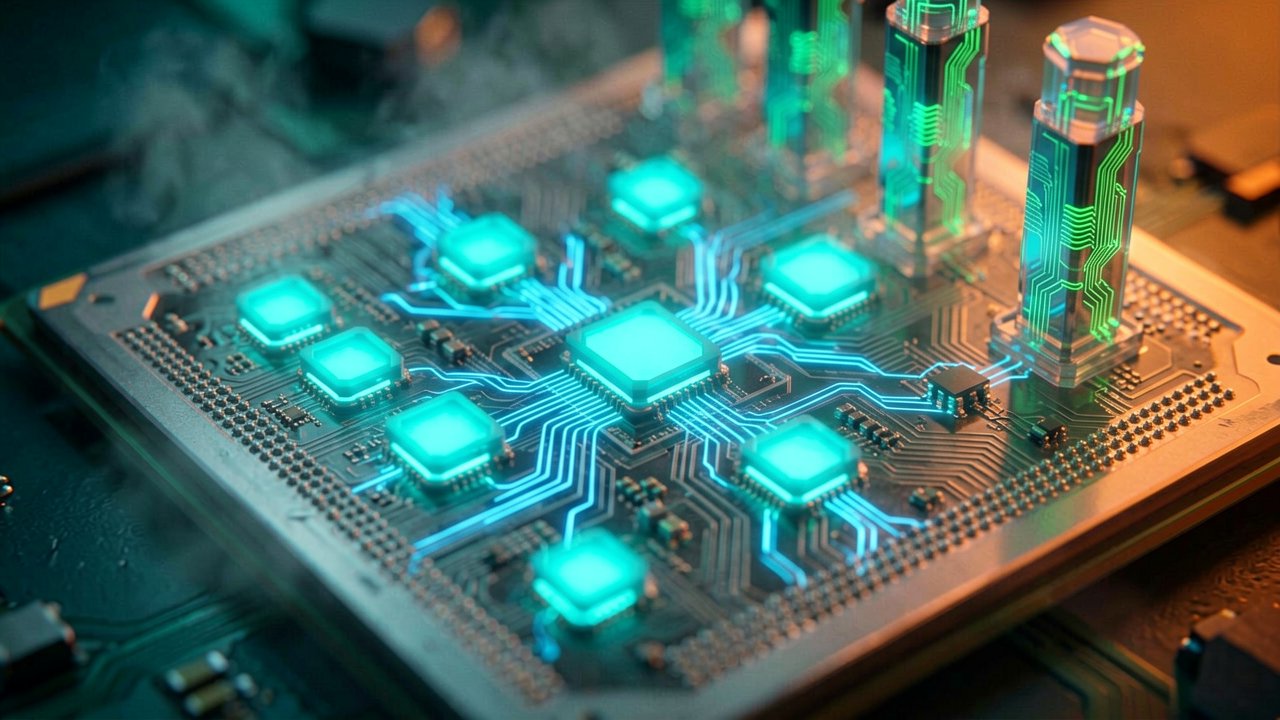
Modern machine learning does not run on general-purpose software; it lives and breathes inside specialized silicon architectures designed to execute trillions of parallel calculations simultaneously. If you peel back the heat sinks of today's dominant artificial intelligence workloads, you will not find the flexible, jack-of-all-trades logic of a standard CPU. Instead, you encounter a highly optimized, relentless processing landscape designed almost exclusively for matrix mathematics. This architectural evolution has shifted the conversation from general clock speeds to specialized throughput, making hardware innovation the true bottleneck—and the true catalyst—for advanced AI scaling.
At the center of this revolution is a fundamental departure from the classic Von Neumann architecture, which spends too much time and energy moving data between memory pools and execution cores. Modern AI accelerators bypass this legacy friction by keeping data in constant motion across massive internal compute arrays. The magic happens within dedicated processing engines like the Matrix Multiply Unit (MXU) found in Google Cloud's tensor processing units. In configurations like the TPU v5p, the system relies on a 128x128 systolic array, an elegant setup where data streams through a network of 16,384 interconnected multiply-accumulate nodes. Data flows through the chip like fluid through a grid, processing weights and activations at every intersection without needing to constantly read from or write back to external registers.
The Physics of Scale and Interconnect
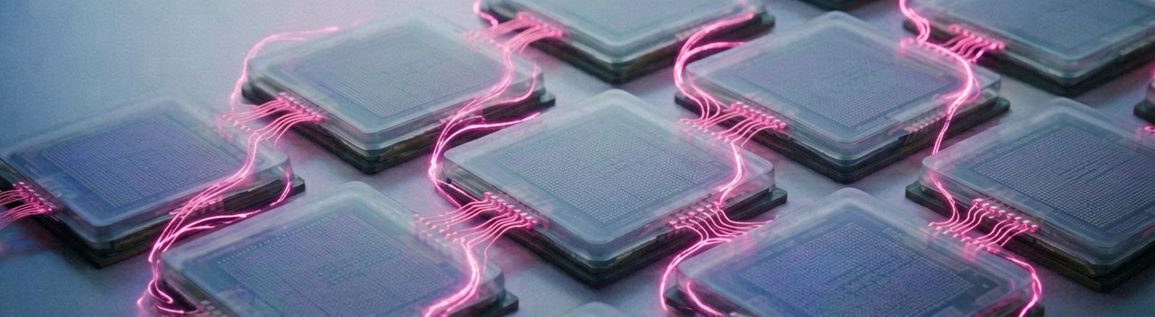
When dealing with modern large language models, a single piece of silicon is never enough. The true test of an accelerator is how well it behaves when tethered to thousands of its peers. The engineering community has responded with high-bandwidth, proprietary fabrics designed to turn massive clusters into a single cohesive supercomputer. While individual processor layouts dictate local math efficiency, custom multi-node fabrics dictate macroscopic performance. This multi-tiered scaling relies heavily on optical circuit switches and dedicated interconnect technologies that dynamically reconfigure cluster topologies based on the specific operational flow of the neural network model being trained.
This design philosophy scales up to monstrous infrastructure footprints, where networking becomes just as vital as internal compute pipelines. For instance, a single pod can scale up to 8,960 interconnected chips via reconfigurable high-speed links, enabling single-slice training for up to 6,144 individual processors according to Google Cloud Documentation . To keep these ravenous mathematical engines fed, hardware architects pack the substrate with high-bandwidth memory (HBM), placing stackable, ultra-wide memory dies directly on the same multi-chip module package to eliminate traditional bus bottlenecks.
Performance Metrics That Matter
Evaluating this new era of silicon requires moving past traditional raw computational ceilings to look at real-world hardware utilization. The raw teraflops quoted on marketing sheets rarely reflect actual workload performance because sparse matrices and data transmission delays frequently force processing elements to sit idle. To combat these bottlenecks, modern architectures introduce specialized hardware components like the "SparseCore" built into Google's tensor architecture to accelerate embedding lookups, ensuring that main math units never stall during recommendation model execution. This clever pairing allows the system to achieve dramatic efficiency improvements, registering a 67% boost in energy efficiency over previous generations despite pushing significantly higher workloads.
Meanwhile, the market's standard for discrete GPUs relies heavily on dynamic precision tuning to squeeze out maximum efficiency per watt. In the fourth-generation Tensor Cores utilized across the NVIDIA Technical Blog specifications, performance leaps are achieved via a specialized transformer engine that automatically manages data precision. This engine dynamically analyzes the requirements of a neural network layer and instantly switches between FP16 and FP8 formats. By dropshipping the math down to 8-bit precision when higher fidelity isn't required, the architecture delivers a staggering 9x faster AI training performance and up to 30x faster inference speedups on massive language workloads compared to older architectural baselines. The future of machine learning isn't just about building larger factories; it's about micro-managing the factory floor at the single-bit level.
Behind the Scenes: The Micro-Architectural Blueprint of Execution
Behind the Scenes: To truly understand why modern deep learning workloads demand specialized silicon, one must look at the hardware-software co-design layers that govern compile-time loop nest transformations. In traditional computing, a central processing unit relies heavily on out-of-order execution, deep branch prediction units, and massive speculative execution pipelines to keep a single, sequential instruction stream moving as fast as possible. Neural networks, by contrast, offer perfect structural predictability. Because the entire network architecture—the layers, tensor dimensions, and activation flows—is known before the first matrix multiplication even begins, systems engineers can strip away almost all control logic hardware and replace it with raw, deterministic arithmetic density.
This structural clarity allows compilers to map mathematical operations directly onto the physical geometry of the silicon substrate. When an open-source compiler framework like XLA receives a model graph, it translates the high-level operators into localized machine instructions through a process called kernel fusion. Instead of writing out intermediate activation tensors to High-Bandwidth Memory (HBM) after a matrix multiply operation, the compiler fuses that multiplication step directly into the subsequent activation function, such as a Rectified Linear Unit (ReLU), entirely within the local SRAM register file. This optimization minimizes memory bandwidth consumption, which remains the single most expensive operation in terms of energy dissipation on a modern die.
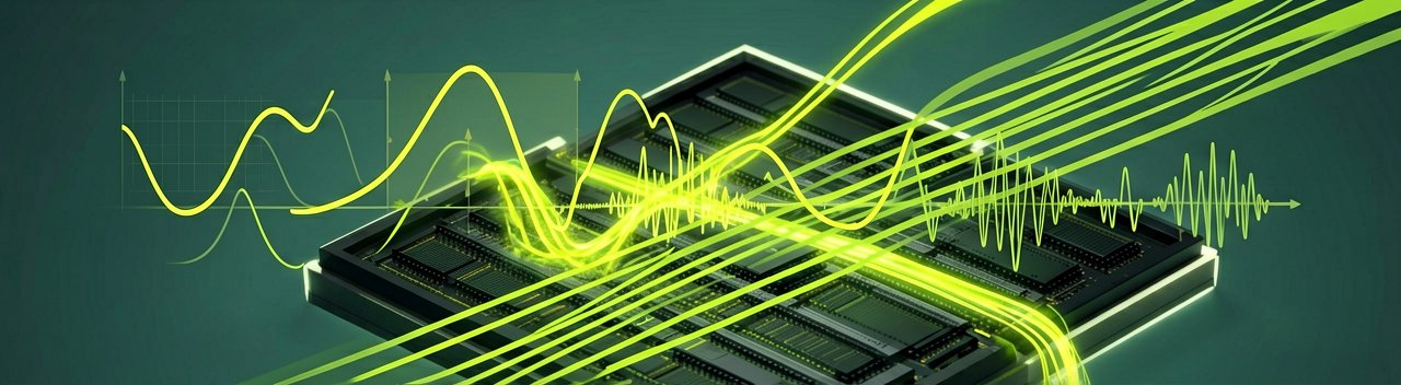
Inside the systolic array itself, timing and synchronization are managed at the single-cycle level through dedicated pipeline registers. Unlike a traditional SIMD (Single Instruction, Multiple Data) execution unit where every arithmetic logic unit reads from a centralized register file simultaneously, a systolic array passes data through adjacent processing elements like a wave. In a standard fused multiply-accumulate loop, weights are loaded from memory into local stationary registers within each node, while activation vectors are shifted horizontally from the left edge of the grid. Simultaneously, partial sums are accumulated and shifted vertically from the top edge downward. By interleaving data movement with calculation, the silicon achieves near-one-hundred-percent utilization of its multiplier circuits, transforming what would be thousands of distinct memory fetches into a continuous, deterministic spatial dance.
To prevent memory latency from stalling this continuous pipeline, engineers deploy asynchronous Direct Memory Access (DMA) engines that run completely decoupled from the main execution units. While the tensor core is crunching through the current matrix tile, double-buffered local SRAM banks are already fetching the next batch of activations from HBM over a massive interposer interface. This masking of memory latency ensures that the computational arrays are never starved for data. On the software side, this requires complex software-managed caching strategies where compilers must precisely predict the exact clock cycle a specific data packet will be required, completely shifting the burden of memory virtualization from runtime hardware controllers to compile-time software logic.
This radical emphasis on deterministic execution fundamentally reshapes the economics of modern machine learning infrastructure. By trading away general-purpose flexibility, hardware architects can pack tens of thousands of arithmetic units into the same physical footprint that would typically hold just a handful of traditional processor cores. Every square millimeter of silicon is optimized to do one thing: multiply and add numbers at a scale that was entirely unimaginable a decade ago. As neural networks continue to expand into hundreds of billions of parameters, this relentless optimization at the hardware-software boundary is the only mechanism capable of keeping the physical energy footprint of global AI training clusters within sustainable boundaries.
Reading Between the Lines: The Structural Illusions of AI Hardware Scaling
Reading Between the Lines: The tech industry has fallen comfortably into the trap of conflating peak theoretical teraflops with true operational efficiency. Silicon marketing departments eagerly parade astronomical performance metrics, yet a closer examination of actual cluster workloads reveals an uncomfortable truth: much of this specialized computing power sits idle, waiting for data to arrive. The industry suffers from a severe memory wall, where the speed of moving data between memory stacks and computational cores lags orders of magnitude behind the processing speed of the arithmetic units themselves. We are building sports car engines but running them on clogged dirt roads, creating a widening chasm between the hardware's theoretical capabilities and its real-world execution efficiency.
This efficiency gap exposes a glaring contradiction in current scaling paradigms. While manufacturers tout the benefits of lower-precision formats like FP8 and INT4 for squeezing more throughput out of silicon, this quantization push introduces a fragile trade-off between hardware performance and model stability. Forcing a multi-billion-parameter neural network into narrower bit widths can lead to unpredictable degradation in reasoning capabilities, catastrophic forgetting, or gradient divergence during training. This creates an adversarial relationship between systems engineers who want to strip precision to save power, and machine learning researchers who require high-fidelity numeric representation to ensure model coherence. The current hardware trajectory forces software to bend to the structural limits of silicon, rather than building architectures that truly serve the algorithmic intent.
Furthermore, the aggressive push toward proprietary, single-vendor interconnect ecosystems poses a significant risk to the broader technology landscape. By tightly coupling hardware layouts to specific, closed-source compiler frameworks, silicon giants are effectively creating walled gardens that stifle architectural diversity. Startups attempting to introduce innovative, non-von Neumann designs face nearly insurmountable software barriers because the modern AI toolchain is heavily optimized for existing tensor core paradigms. If the industry continues down this path of hyper-specialization, we risk locking ourselves into a local maximum, optimizing a single way of computing while starving alternative, potentially superior AI architectures of the hardware support they need to mature.
Looking ahead, the environmental and economic realities of this silicon arms race will eventually demand a reckoning. The trajectory of scaling clusters to tens of thousands of power-hungry chips is fundamentally unsustainable from an infrastructure perspective. We are rapidly approaching the physical limits of power delivery and thermal dissipation on standard chip packages, forcing data centers to morph into complex liquid-cooled power plants just to keep the lights on. The next breakthrough in machine learning capability will likely not come from simply stacking more silicon wafers together, but from architectural paradigms that radically rethink data locality and sparse execution from the ground up.
"We have spent the last decade building silicon cathedrals dedicated to the holy matrix multiplication, only to realize that the most expensive part of modern artificial intelligence is still the electric bill."
Artūras Malašauskas is an AI Systems Integrator with 20+ years of production-grade web engineering experience. He has designed, shipped, and scaled enterprise Python/PHP systems for logistics, SaaS, and public-sector clients. For the past year, he has focused exclusively on AI integrations: deploying open-source LLMs, building generative media pipelines (image, audio, video), and engineering multi-agent workflows for real production environments. His standard: reproducibility, security, cost-efficient inference—no vaporware. He documents and evaluates emerging AI tooling, separating verified capabilities from marketing noise. Technical editor at: muza-ai.eu, ai-verslas.lt, ai-naujinos.lt Connect on LinkedIn
Comments