STMicroelectronics Disrupts Edge AI Dynamics with Miniature 2.3K-Zone LiDAR Module
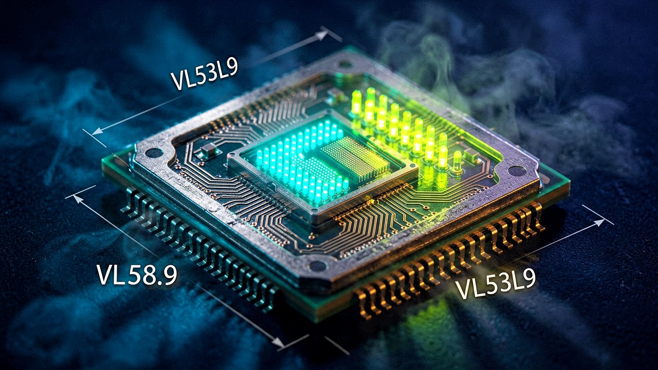
For a long time, embedding high-resolution spatial awareness into compact, power-constrained hardware felt like trying to squeeze a theater-sized projector into a coin purse. Tech teams designing the next wave of autonomous hardware typically slammed into a brick wall of component complexity, relying on bulky discrete sensors that demanded complex, manual calibration. The latest silicon coming out of Europe completely shatters this compromise. According to an official press release hosted on GlobeNewswire , STMicroelectronics has launched the VL53L9, a direct Time-of-Flight (dToF) 3D LiDAR all-in-one module that brings massive spatial intelligence to edge AI networks without turning the host device into a power hog or an engineering nightmare.
The hardware architecture here reveals serious micro-engineering magic. STMicroelectronics managed to pack a massive Single Photon Avalanche Diode (SPAD) sensor array, an on-chip dToF processing ASIC, an embedded power management IC (PMIC), and dual vertical-cavity surface-emitting lasers (VCSELs) into a tiny, reflowable package measuring just 12.8 mm x 6.1 mm x 4.6 mm. But the real structural differentiator is the introduction of a new metasurface optical element alongside unique dual-scan flood illumination. As detailed on the official STMicroelectronics Blog, this flood scanning system entirely replaces old-school dot-scanning configurations, enabling much tighter contour mapping around tricky, slender edges and cutting down motion artifacts that usually confuse low-power systems. Because everything sits natively on the silicon, developers get a calibration-free sensor straight out of the box, throwing the typical hardware alignment headaches completely out the window.
Uncompromising Performance at the Bare Edge
When looking at the hard metrics, the silicon delivers spatial data that previously required discrete, expensive sensor stacks. The hardware pipes an unprecedented 2,268 resolution zones across a 54° x 42° field of view, establishing a sharp 1° angular resolution that lets small microcontrollers easily tell a flat wall apart from a moving human limb. It tracks targets spanning from a mere 5 centimeters up to a distant 9 meters, all while holding a tight 1% accuracy margin. For systems that cannot afford a millisecond of lag, like collision avoidance in consumer drones or real-time gesture tracking in mixed-reality gear, the VL53L9 streams processed 2D infrared images and depth maps at a blistering 60 frames per second, which can scale up to 100 Hz over a high-bandwidth MIPI or I3C interface. Best of all, the on-chip processing swallows the heavy, math-intensive histogram calculations locally, which drops the typical computational load off external RAM and lets complex edge AI operations thrive on budget-friendly microcontrollers drawing very little power.
Behind the Scenes: Under the Hood of Zero-Latency Spatial Processing
For systems engineers tasked with squeezing real-time spatial awareness out of low-power microcontrollers, the true genius of the VL53L9 lies in its hardware-accelerated histogram processing pipeline. In traditional direct Time-of-Flight configurations, calculating depth requires streaming raw photon-arrival timetags over an external bus to a host processor, causing immediate memory bottlenecks and severe CPU thrashing. STMicroelectronics circumvents this entirely by embedding a dedicated hardware ASIC directly onto the sensor die. This specialized silicon handles real-time ambient light subtraction, multi-object detection, and raw distance computation locally, spitting out clean, pre-calculated depth frames rather than noisy, raw data streams. By treating spatial processing as an autonomous background task, the system completely frees up the main application processor to run deep edge AI networks instead of wasting precious clock cycles on basic sensor filtering.
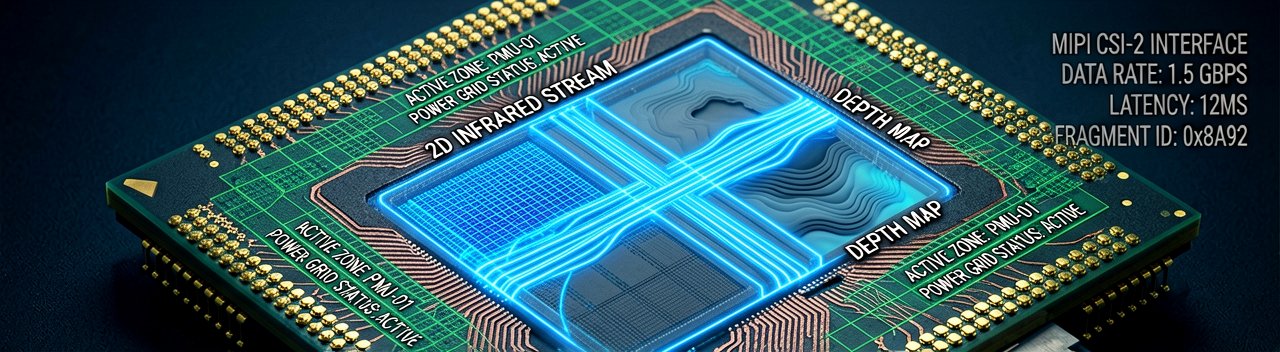
Architecturally, managing a massive 2,268-zone matrix demands a radical departure from standard memory bus topologies. The module relies on an ultra-compact, high-speed interface supporting both MIPI CSI-2 and I3C protocols, providing a direct pipeline to feed dual data formats straight into the host's direct memory access (DMA) buffers. The sensor simultaneous outputs a processed 2D infrared intensity image alongside the 3D depth map, mapped directly in a synchronized frame format. This dual-stream approach is a goldmine for computer vision applications. Because the 2D visual data aligns precisely with the 3D spatial grid at the hardware layer, developers can implement multi-modal sensor fusion algorithms—such as pairing an infrared contrast map with raw depth data for low-light face authentication—without needing computationally expensive coordinate transformation matrices or frame-alignment software routines.
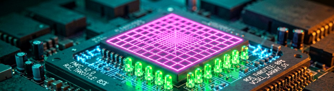
Power budgeting is another area where this architectural efficiency pays massive dividends for mobile and battery-operated edge systems. The integration of an on-chip power management IC (PMIC) allows the sensor to switch dynamically between localized region-of-interest (ROI) scanning and full-frame dual-scan flood illumination. Instead of firing all vertical-cavity surface-emitting lasers (VCSELs) at a constant, power-hungry duty cycle, the system allows the host controller to programmatically isolate specific zones down to an individual cluster level. When the edge AI detects zero motion in the periphery, it throttles down the inactive zones, instantly slashing the sensor's power draw while maintaining a high-frequency refresh rate on the critical tracking target. This fine-grained control turns spatial mapping into a dynamic, software-defined resource that scales power consumption linearly with environmental activity.
Reading Between the Lines: The Reality of High-Density Spatial Scaling
While a 2.3K-zone LiDAR sensor packaged into a footprint smaller than a fingernail sounds like a slam dunk for the robotics industry, deploying this hardware in the messy, uncalibrated real world introduces a distinct set of engineering challenges. Industry hype often conflates raw pixel count with practical, actionable resolution. In truth, splitting a 54-degree field of view into thousands of discrete zones means each individual Single Photon Avalanche Diode (SPAD) cluster receives only a tiny fraction of the returning laser energy. When operating in pristine, indoor laboratory conditions, the return signal is perfectly clear; however, the moment this sensor steps outside into blinding 100,000-lux ambient sunlight, the signal-to-noise ratio faces an aggressive uphill battle that localized hardware histograms can only partially mitigate.
There is also a subtle contradiction in the way edge AI silicon is marketed versus how it must actually be implemented in production. STMicroelectronics rightfully prides itself on offloading the primary dToF calculations onto the module's internal ASIC to save host CPU cycles. Yet, the sheer velocity of streaming synchronized 2D infrared images and 3D depth maps at 60 to 100 Hz creates an immense data firehose that low-power microcontrollers are fundamentally ill-equipped to ingest. A systems architect cannot simply plug this sensor into a standard, ultra-low-power Cortex-M4 node and expect seamless object recognition. The reality is that the data ingest bottlenecks are merely shifted from the computation stage to the communication bus, demanding advanced, high-bandwidth I3C or MIPI routing that drives up PCB complexity and development costs.
Looking at the broader market, the miniaturization of high-density LiDAR will inevitably trigger an architectural arms race at the software layer. As hardware barriers collapse and spatial sensors become cheap, commoditized components, the engineering bottleneck shifts entirely to the quality of the edge AI algorithms parsing the depth data. The industry must move away from heavy, power-hungry neural networks toward sparse, event-driven vision models that can actually capitalize on a 1-degree angular resolution without melting a device's battery pack. Until the software ecosystem catches up to this rapid hardware shrinkage, many teams risk over-specifying their sensor arrays only to filter out ninety percent of the rich spatial data just to keep their systems from overheating.
Designing for the edge is the art of celebrating a breakthrough in micro-silicon packaging, only to realize you now have to explain to management why your ten-dollar microcontroller is choking on a beautifully precise, high-speed flood of spatial data it never actually had the memory to digest in the first place.
Artūras Malašauskas is an AI Systems Integrator with 20+ years of production-grade web engineering experience. He has designed, shipped, and scaled enterprise Python/PHP systems for logistics, SaaS, and public-sector clients. For the past year, he has focused exclusively on AI integrations: deploying open-source LLMs, building generative media pipelines (image, audio, video), and engineering multi-agent workflows for real production environments. His standard: reproducibility, security, cost-efficient inference—no vaporware. He documents and evaluates emerging AI tooling, separating verified capabilities from marketing noise. Technical editor at: muza-ai.eu, ai-verslas.lt, ai-naujinos.lt Connect on LinkedIn
Comments