Silicon Shake-Up: Inside Samsung’s Exynos 1680 Tech Evolution

Samsung’s mobile silicon division isn't content letting premium features stay exclusive to four-figure flagships. The newly unveiled Samsung Semiconductor Exynos 1680 signals an aggressive push to bring high-end computational and photography muscle deeper into the mid-range market. Fabricated on a refined 4-nanometer node, the chipset represents a calculated hardware recalibration aimed directly at driving demanding on-device AI tasks and sprawling, high-megapixel camera sensors without burning through a phone’s battery life by lunchtime.
The structural headline here is Samsung’s upgraded tri-cluster CPU configuration. Unlike typical mid-tier designs that skimp on raw muscle, the Exynos 1680 deploys an intentional 1+4+3 core topology to balance sustained throughput and passive efficiency. It pairs a single, high-frequency Cortex-A720 prime core running at 2.9GHz with four mid-tier Cortex-A720 performance cores clocked at 2.6GHz, leaving the grunt work of background tasks to three power-sipping Cortex-A520 efficiency cores running at 1.95GHz. By shifting one core from the efficiency tier over to the mid-performance cluster compared to older layouts, the hardware yields a far more responsive system during heavy application switching and intensive multitasking loops.
Graphics, AI, and Next-Gen Computational Thermals
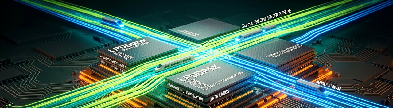
On the visual front, the architecture integrates a customized Samsung Xclipse 550 GPU co-developed with AMD and built on the modern RDNA 3 microarchitecture. According to reports tracked by Gadgets360, this design tweak unlocks a 16% uplift in graphics rendering capability over the previous generation, optimizing frame consistency in popular mobile titles while maintaining unusually low thermal output during extended gaming stress tests. This graphics processing unit works alongside an upgraded neural processing unit capable of outputting 19.6 trillion operations per second (TOPS), laying down the computational track needed to execute real-time language translations and photo manipulation natively on the device.
Flagship-Grade Optics Meet Fast Storage
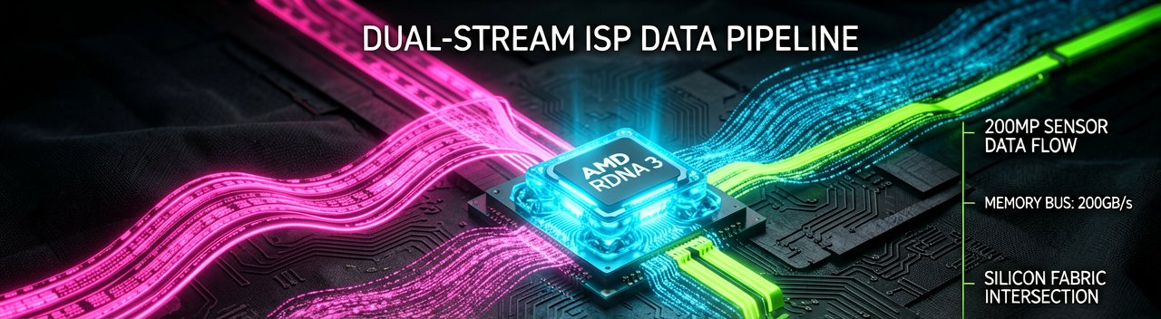
Where the Exynos 1680 truly punches above its weight class is inside its rewritten Image Signal Processor. The hardware proudly claims native compatibility with massive 200-megapixel camera sensors, matching the raw input capabilities of top-tier mobile devices. This robust ISP architecture guarantees rapid multi-frame noise reduction, sharper details in low-light environments, and 4K video recording capped at a fluid 60 frames per second with 10-bit HDR depth. Data bottlenecks are actively countered across the rest of the board through native support for ultra-fast LPDDR5X memory arrays and UFS 4.1 onboard flash storage, keeping the pipeline completely open for high-bandwidth data transfers.
Connectivity suites round out the platform with an integrated 5G modem pushing theoretical sub-6GHz download thresholds up to 5.1Gbps, as highlighted by Gadget Bridge. Modern wireless standards like Bluetooth 6.1 and Wi-Fi 6E are baked natively into the silicon, making sure peripheral pairing and network handshakes don't cause systemic performance stutters. By stitching together high-end optical support, an ambitious tri-cluster core division, and a highly optimized GPU layout, Samsung's newest mid-range silicon platform successfully narrows the performance divide that traditionally separates daily drivers from absolute luxury devices.
Behind the Scenes: Building a mid-range platform with flagship ambitions forces silicon engineers to rewrite the rules of data movement. At the systems architecture level, the primary enemy of sustained performance is memory wall latency. To prevent the single Cortex-A720 prime core from starving during intensive tasks, Samsung engineered a unified L3 cache structure paired with an optimized dynamic voltage and frequency scaling algorithm. Rather than relying on rigid performance states, the chip's internal power management integrated circuit monitors kernel schedulers at a microsecond level. This allows the system to instantly shunt critical rendering threads to the high-performance cluster while dynamically parking the efficiency cores to protect the chip's thermal envelope.
Low-Level Execution and Neural Architecture
The system-on-chip handles intensive AI workloads by moving beyond standard linear matrix multiplications. The 19.6 TOPS neural processing unit leverages a proprietary hardware block engineered specifically for mixed-precision quantization. When processing real-time imaging data or large language models, the compiler dynamically switches execution pipelines between INT8, INT16, and FP16 math based on the required accuracy threshold. This adaptive precision pipeline prevents memory bandwidth saturation by compressing weight matrices directly in the hardware, ensuring that local AI models execute with minimal cache misses and lower overall instruction overhead.
Memory subsystem optimizations play a equally critical role in maintaining the fluidity of the user interface under heavy loads. The inclusion of LPDDR5X support brings an advanced low-power auto-refresh mechanism that operates down to the individual bank level. By executing localized refreshes rather than locking the entire memory bus, the memory controller cuts idle power consumption significantly while freeing up instantaneous bandwidth for the Xclipse 550 GPU. When the AMD RDNA 3-based GPU requests heavy vertex and texture data during 3D rendering, the memory bus utilizes an optimized command queue prioritization system to prevent display pipeline stuttering.
Sustaining 200MP Throughput Without Bottlenecks
Handling the raw pixel stream from a 200-megapixel camera sensor requires massive structural changes to the traditional Image Signal Processor pipeline. The Exynos 1680 utilizes a parallel dual-stream ISP architecture that splits the massive incoming image payload into distinct, manageable data columns. These columns are processed simultaneously across specialized hardware accelerators designed for zero-shutter-lag operations. To manage this massive data influx without overflowing the system cache, the ISP writes directly to a dedicated, high-speed buffer before handing the uncompressed frame data over to the hardware encoder for final compression.
Underneath the hood, the silicon relies on an updated hardware-level interconnect designed to minimize internal data routing bottlenecks. This intra-chip fabric acts as a high-speed highway, linking the tri-cluster CPU, the AMD-powered GPU, and the dual-stream ISP directly to the system's global memory cache. By implementing a sophisticated Quality of Service protocol across this internal fabric, the hardware ensures that critical time-sensitive data, like real-time display refresh cycles or audio tracking streams, always receives priority over background file writes or network synchronization tasks.
Reading Between the Lines: Jamming flagship specifications into a mid-tier marketing brochure is an ancient industry tradition, and the Exynos 1680 requires a healthy dose of analytical skepticism. While a 200-megapixel camera capability sounds groundbreaking for an affordable device, it creates a massive engineering contradiction. A sensor of that scale captures an overwhelming volume of raw data, yet the mid-range silicon platform lacks the massive memory bus width and massive system caches found in premium tier chips. This mismatch means users will likely face noticeable processing delays between shutter presses, turning what looks like a flagship photography experience into a lesson in patience while the hardware struggles to clear its image buffer.
The Realities of the Tri-Cluster Trade-off
The shifted 1+4+3 tri-cluster CPU configuration also invites scrutiny regarding long-term thermal sustainability. By allocating five out of eight total cores to heavy-lifting performance tasks, Samsung has noticeably skewed the power budget toward peak performance rather than steady-state efficiency. In short bursts, this layout will feel remarkably snappy and responsive. However, in slim mid-range phone chassis that typically lack advanced vapor chamber cooling systems, this configuration runs the risk of hitting thermal ceilings quickly, forcing the aggressive power management algorithms to throttle clock speeds down to basic levels during extended use.
Furthermore, the heavily promoted 19.6 TOPS NPU sits in a complex development ecosystem that rarely favors mid-range hardware. Most mobile software developers optimize their on-device AI models for either top-tier flagship silicon or the lowest common denominator to maximize market reach. A mid-market chipset introducing a unique mixed-precision architecture faces an uphill battle in attracting developer optimization, which means that impressive theoretical performance metric may largely translate to wasted silicon area that rarely sees real-world utilization outside of Samsung's own stock applications.
Market Positioning and the Performance Illusion
This tactical balancing act reveals a broader strategic play by Samsung Semiconductor to redefine what constitutes value in a tightening smartphone market. By packing highly visible features like AMD RDNA 3 graphics architecture and ultra-high-resolution imaging support into mid-tier silicon, they successfully muddy the waters between true premium devices and upper-mid-range alternatives. It is a calculated gamble that relies on consumers prioritizing impressive hardware specifications over sustained, real-world execution metrics under heavy, prolonged workloads.
Ultimately, the Exynos 1680 behaves less like a democratized flagship processor and more like a highly optimized exercise in compromise. It delivers undeniable upgrades in burst computational speed and modern connectivity standards, but it remains tethered to the economic realities of its product segment. The success of the architecture will not be measured by its theoretical top-end performance capabilities on a test bench, but by how gracefully its aggressive thermal and memory constraints hold up when real-world users push the hardware beyond its comfort zone.
Designing mobile silicon is a lot like packing a suitcase for a weekend trip: you can try squeezing in a premium tuxedo and scuba gear, but eventually, the zippers of the mid-range budget are going to scream for mercy.
Artūras Malašauskas is an AI Systems Integrator with 20+ years of production-grade web engineering experience. He has designed, shipped, and scaled enterprise Python/PHP systems for logistics, SaaS, and public-sector clients. For the past year, he has focused exclusively on AI integrations: deploying open-source LLMs, building generative media pipelines (image, audio, video), and engineering multi-agent workflows for real production environments. His standard: reproducibility, security, cost-efficient inference—no vaporware. He documents and evaluates emerging AI tooling, separating verified capabilities from marketing noise. Technical editor at: muza-ai.eu, ai-verslas.lt, ai-naujinos.lt Connect on LinkedIn
Comments