The $400 Million Leap: ASML’s High-NA Machines Are About to Drop Their First Real Chips
The semiconductor world moves on a razor's edge, and ASML just gave us a definitive timeline for the next big shift. Chief Executive Christophe Fouquet confirmed on Tuesday that the first chips manufactured with the company's next-generation High-NA (High Numerical Aperture) EUV machines will arrive in just a few months. Speaking at an industry conference in Antwerp, Fouquet made it clear that despite the eye-watering $400 million price tag per unit, these behemoths are no longer just expensive science experiments—they’re moving into the active fabrication phase for both memory and logic products. According to reports from Reuters , this marks a critical milestone for a technology that many feared might be delayed by its own complexity and cost.
While the hardware is technically a marvel, the industry remains split on how quickly to dive into the deep end. Intel has been the loudest cheerleader, aggressively integrating High-NA tools into its 14A node development in a bid to reclaim the manufacturing crown. On the flip side, TSMC—the world’s largest contract chipmaker—has played it safe, recently suggesting the machines might be too expensive for the current generation's ROI. But as The Economic Times notes, the sheer demand for AI-capable silicon is forcing the hand of every major player. Fouquet’s "within months" prediction suggests that early-stage production or "exposed" wafers are imminent, likely coming from the R&D lines at places like Intel or the imec research hub itself.
The Math Behind the Mirror
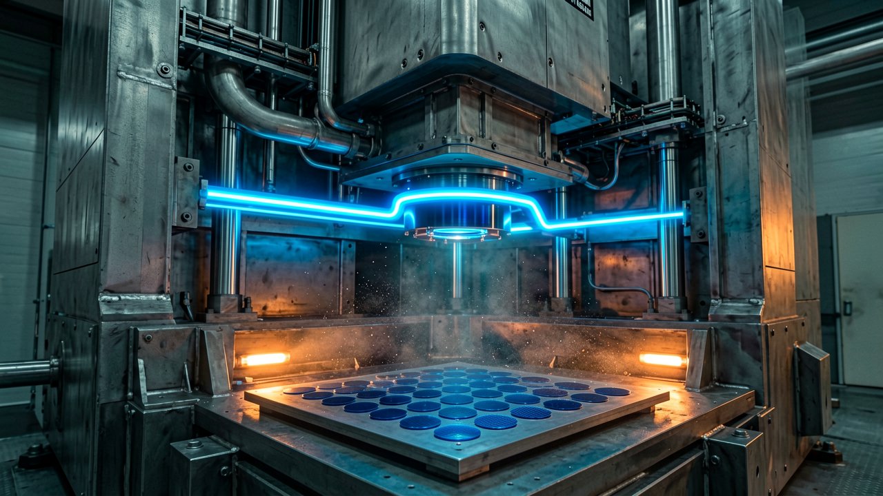
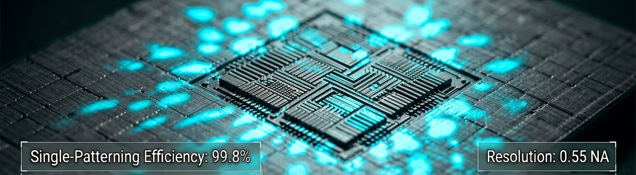
The technical "magic" of High-NA boils down to resolution. By increasing the numerical aperture from 0.33 to 0.55, ASML’s machines can print features 1.7 times smaller than current EUV tools, allowing for nearly triple the transistor density in a single exposure. This isn't just about making things smaller; it’s about avoiding the "multi-patterning" headaches that slow down production and introduce errors. According to technical deep-dives at Tom's Hardware, each machine is a logistics nightmare, weighing 150,000 kilograms and requiring 250 shipping crates just to move. Yet, for chipmakers looking to hit the sub-2nm mark, there simply isn't another way forward.
The stakes couldn't be higher for the Dutch firm, which effectively holds a monopoly on the extreme ultraviolet lithography needed for modern electronics. While skeptics point to the skyrocketing costs of each successive generation, ASML is betting that the AI boom will provide the necessary capital for its customers to upgrade. If these first chips perform as promised later this year, the pressure on holdouts like TSMC to accelerate their own adoption will likely reach a fever pitch.
Behind the Silicon Curtain: The High-Stakes Gamble of High-NA
The Trillion-Dollar Squeeze: What most surface-level reports miss is the sheer physical audacity required to move the needle in lithography. We aren't just talking about a better lens; we are talking about a total re-engineering of the light path. ASML’s move to High-NA required a complete departure from the previous "Step-and-Scan" architecture to a "High-Numerical Aperture" system that uses anamorphic optics—mirrors that magnify differently in two directions. This isn't just a technical footnote. For the fabs, it means their entire floor plan has to change. These machines are taller, requiring deeper cleanroom ceilings, and the massive amount of power they draw necessitates a localized grid upgrade that few companies can afford without a guaranteed market for the end product.
Historical context tells us that being first isn't always a victory lap. Intel’s aggressive stance today is a mirror image of their hesitation a decade ago. Back then, Intel bet against the first generation of EUV, opting to stick with double-patterning DUV techniques while TSMC and Samsung dived into the EUV deep end. That single decision cost Intel its decade-long lead and forced a multi-year turnaround strategy under Pat Gelsinger. Now, Intel is paying any price—including the rumored $400 million per unit—to ensure they are the ones holding the keys to the first High-NA production line. They are effectively betting the company's "five nodes in four years" roadmap on ASML’s ability to deliver stable uptime on these first units.
TSMC’s current public hesitation is equally calculated. While ASML’s Christophe Fouquet is pushing the "months, not years" timeline, TSMC’s C.C. Wei has been more pragmatic, noting that the cost-to-performance ratio for High-NA might not make sense for their customers until 2026 or later. TSMC has mastered the art of squeezing every ounce of life out of existing hardware. By using "standard" EUV with complex multi-patterning, they can achieve similar density results for their 2nm process without the massive capital expenditure of the new machines. This creates a fascinating divergence in the industry: a race between Intel’s raw hardware superiority and TSMC’s refined process efficiency.
The memory sector is the quiet dark horse in this race. While logic chips for AI and CPUs get the headlines, DRAM manufacturers like SK Hynix and Samsung are looking at High-NA as a way to simplify their increasingly messy layering processes. The transition to High-NA allows these companies to print critical layers in a single pass, which significantly boosts yield. In a market where margins are razor-thin, a 5% increase in yield because of a more precise machine can actually pay for that $400 million price tag faster than a high-end AI processor can. This explains why Fouquet specifically highlighted "memory" alongside logic in his recent remarks.
Ultimately, the "within months" arrival of these chips is a stress test for the entire global supply chain. It isn't just about the machine; it’s about the "resists"—the chemicals used to coat the wafers—and the "masks" that must be defect-free at a scale that was previously impossible. If the chemistry doesn't keep up with the physics of the High-NA light, even the most expensive machine in history becomes a very large paperweight. The next quarter will prove whether the ecosystem is ready to handle the intensity of 0.55 NA light or if we are looking at a longer period of expensive calibration before these machines truly drive the next AI revolution.
The Diminishing Returns of Atomic Precision
Reading Between the Lines: The celebratory tone surrounding the "imminent" arrival of High-NA chips masks a cold, uncomfortable reality regarding the physics of profit. We have reached a point where the cost of lithography is scaling faster than the performance gains it provides. For decades, Moore’s Law was driven by clever engineering that actually made chips cheaper per transistor. Today, ASML’s $400 million price tag represents a decoupling of that economic law. We are moving into an era of "brute force" scaling, where only a handful of trillion-dollar entities can even afford to participate in the game, effectively turning the semiconductor frontier into a gated community for the tech elite.
There is also a glaring contradiction in the industry’s timeline versus its infrastructure. While ASML is confident in the delivery of the machines, the broader ecosystem—the photoresists, the metrology tools, and the high-energy power systems—is still in a state of catch-up. Using a High-NA machine with current-generation resists is like putting racing fuel into a sedan; you might get a burst of speed, but the system isn't designed to handle the heat. Skeptics suggest that these first chips arriving "in months" will likely be low-yield engineering samples or specialized test vehicles rather than the high-volume silicon destined for your next smartphone. The gap between a successful "exposure" and a commercially viable product line remains a chasm that marketing departments often overlook.
Furthermore, the geopolitical weight of these machines cannot be ignored. ASML is no longer just a company; it is a strategic bottleneck in the global cold war over AI. By accelerating the rollout of High-NA, ASML is essentially dictating which nations remain relevant in the compute race. If the technical hurdles of High-NA prove more stubborn than anticipated, the ripple effects will be felt not just in Silicon Valley, but in national security briefings in Washington and Beijing. The margin for error has shrunk to the width of a single atom, and any delay in the "months" promised by Fouquet could stall the projected growth of the entire generative AI sector, which has already priced these hardware advancements into its multi-year valuations.
We must also consider the "Hyper-NA" shadow looming on the horizon. Even as the industry struggles to digest the cost and complexity of the 0.55 NA systems, ASML is already discussing the next leap to 0.75 NA. This constant state of transition creates a perpetual "buyer's remorse" cycle for manufacturers. TSMC’s hesitance to adopt High-NA immediately might not be a lack of ambition, but rather a sophisticated hedge. If they can skip the most painful parts of the High-NA learning curve and jump straight to a more mature version of the process, they could theoretically maintain their dominant margins while Intel absorbs the "pioneer tax" of being the first to break new ground.
Ultimately, the arrival of these chips signals the end of the "easy" era of semiconductors. Every nanometer gained from here on out will be bought with billions of dollars and monumental amounts of electricity. The industry is betting that the world’s thirst for AI is unquenchable enough to justify these costs, but if the AI bubble shows even a hint of stabilization, the financial weight of these High-NA machines could become a localized gravity well for the companies that over-leveraged to buy them. We are watching a high-stakes game of poker where the chips are made of silicon and the buy-in is the GDP of a small country.
Building a machine that can print features the size of a virus on a piece of sand for the price of a Boeing 747 is a monumental achievement, provided you have a customer who doesn't mind paying thirty dollars for a digital toaster that can think for itself.
Artūras Malašauskas is an AI Systems Integrator with 20+ years of production-grade web engineering experience. He has designed, shipped, and scaled enterprise Python/PHP systems for logistics, SaaS, and public-sector clients. For the past year, he has focused exclusively on AI integrations: deploying open-source LLMs, building generative media pipelines (image, audio, video), and engineering multi-agent workflows for real production environments. His standard: reproducibility, security, cost-efficient inference—no vaporware. He documents and evaluates emerging AI tooling, separating verified capabilities from marketing noise. Technical editor at: muza-ai.eu, ai-verslas.lt, ai-naujinos.lt Connect on LinkedIn
Comments